アナログトランジスタはデジタル3,000個分の価値がある
 アナログとデジタルの境界を超
著者は、ハードウェアとソフトウェアの関係性に着目し、デジタル計算機の限界を指摘する。
アナログ回路を用いた新しい計算手法の可能性について述べ、実際の回路設計や技術例を交えて説明している。
ソフトウェアとハードウェアの関係についての深い洞察が語られる。筆者が主張するのは、アナログコンピューティングの重要性であり、デジタルに依存しない新たなコンピューティングの可能性を提示している。
コンピューティングの定義とデジタルの限界
コンピューティングは、コンピュータで行われるあらゆる操作を指すが、多くの場合デジタル論理に限定されがちだ。筆者はこの狭義の理解に疑問を投げかけ、自然現象や生物学でもコンピューティングが行われていると指摘している。
アナログコンピューティングの利点
アナログでは、加算や微分方程式の解法などは効率的だが、デジタルの利点であるプログラマビリティや低消費電力は知られていなかった。アナログにプログラマビリティを導入することで、スケーラビリティが向上し、デジタルの利点を活用できる可能性がある。
実現可能なアナログコンピューティングの例
FGトランジスタなどの成熟した技術を用いることで、実際のデバイスが実現可能であることを示している。筆者は、実際のデバイスや研究をもとに、アナログコンピューティングの可能性を説明している。
まとめ
アナログコンピューティングは、デジタルに依存しない新たなコンピューティングの可能性を示しており、今後の技術革新に期待が寄せられている。
原文の冒頭を表示(英語・3段落のみ)
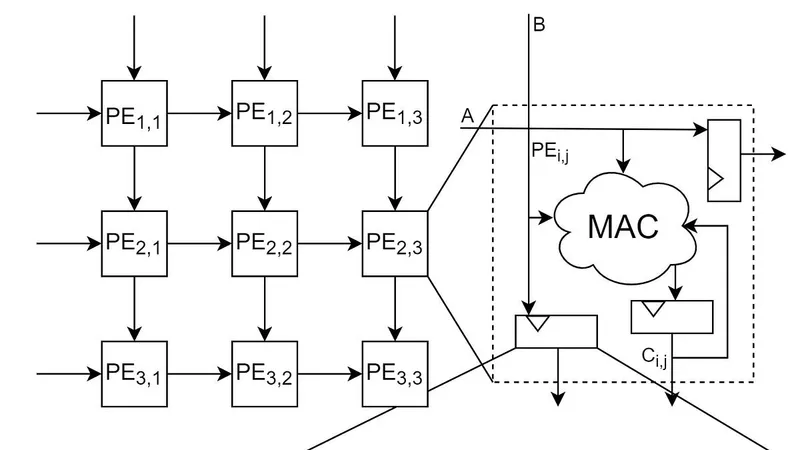
The interesting thing to me about software was the infinite canvas it presented in tension with the speed of light constraints that the hardware might impose. While on the one hand, a digital landscape presents infinite possibilities, on the other hand the effectiveness to which that could be created, packaged and enjoyed by any size audience (1 person – 10B+) depends on the computer where the operations occurred. This description is deliberately abstract because the history of computing spans from analog modes of counting to mechanical devices predicting the tides to modern city-scale datacenters to the distributed billions of edge devices that dwarf any past/current aggregated datacenter capacity. However, the rhetorical trick I’m pulling here is assuming we have a shared understanding of that word “computing”. Many widely available definitions simply state that it is any operation done on a computer and similarly computers are seen as firmly the domain of digital logic. This is where my first disagreement with colloquial understanding starts to become apparent. I am very far from the first person to point out that many natural phenomena and biology achieve similar goals of computing without being tied to the digital domain, but it allows us to circle back to why the relationship of hardware to software is so interesting. The hardware and its primitives shape the incentives and outcomes of the software (as nicely put by Hooker in The Hardware Lottery). If you have different hardware you can end up with stars, the cosmos, geology. These are not “operations” or programs people might usually associate with how primitives of a computer shape the outcome but this unconventional view circles around the point I’m driving towards. The field of Neuromorphic engineering might argue that biological life is also downstream of this alternative hardware stack. Ultimately my goal here is to ease us into the large, wonderful world of physical computing which is the superset that encompasses optical, analog, quantum, digital, biological and every other branding term in between. A thorough discussion of the tradeoffs that each one makes as they pick different primitives, principles, architectures or theoretical basis exceeds the space for any single discussion. And personally, I don’t feel comfortable attempting to do justice to those outside of analog and digital computing at the moment. But by constraining the discussion to those two, we can compare what is possible today, what has been experimentally validated, what you can recreate with simulations at home and just how much more we could be getting out of our transistors if we break out of the digital Von Neumann world.For the purposes of this discussion how would we define analog computing? The process of treating transistors (or other computing primitives) as continuous devices which can be wired together and applied towards implementing an operation. This itself is not new as the history of analog circuit design is beautiful, varied and deep. It has long been known that basic operations like summation, differential equation solvers, integration or slightly more complex ones like filtering & multiplication are more efficient in the analog domain. What is less widely known is how to make computing with analog circuits scalable. Even without having any circuit background it is possible to see the immediate advantage a digital circuit has over an analog one is that the digital one only has two states to worry about; 0 or 1. The analog world must care about 0 to 1 (to a yet unspecified level of precision). Another seemingly “core” advantage of the digital world is its programmability. Digital memory, registers, can switch its state at will that change the outcome of the operation. Now what if we could roll all of these seeming digital advantages into the analog domain? Programmability that grants the ability to cleanly maintain states in between 0 and 1 which in turn allows many analog circuits previously plagued by mismatch to act similarly. This grants scalability to the analog domain. Now there is no free lunch in life (if you find some, send me an email!) there are absolutely different constraints to deal with in such a paradigm but knowing such a thing is possible we can ask why would we do it? Well for starters how does 100-1000x power reduction sound? Followed by a much smaller area due to single transistor multiplies, “free” addition from current summation and reprogrammable analog circuits post fabrication without large, external resistors? When I’m discussing this in real life its usually at this point I like to stress that I’m not selling you on a theoretical future that could exist but rather on research, chips and real working platforms that I and those before me have built. The next question is how do you realize these ideas? While I’m partial to the transistor there are many options for a primitive: memristors (ReRAM, Phase Change Memory -PCM etc), Spin Orbit Torque Magnetic Tunnel Junctions (SOT-MTJs), Ferro Electric Field Effect Transistors (FEFETs) and many other exciting emerging devices. However, I return to specifically floating-gate (FG) transistors due to their maturity (if you use SSDs, SD cards or modern phone storage you’ve relied on FGs!) and experimental demonstrations (each link here is different) over the years as the suitable primitive for programmable analog computing. But enough jawboning about analog computing this and power improvement that I think the best way to show not just tell is walking through examples. In fact, my initial goal of writing or future content is to spend time implementing these concepts for a broader audience.As motivation for interesting problems to tackle today, I’ll be using the Dwarkesh/Reiner interview that walks through the basics of operations in an “AI” chip. Please check it out if you haven’t but essentially Reiner walks Dwarkesh through logic gates involved in machine learning accelerators among other interesting topics.# The MAC in Matrix OperationsThe first thing discussed is realizing a multiply accumulate (MAC) operation in the digital domain. Simply put: multiply two numbers and either add it to a running sum or a third number. This is the perfect starting point as it’s the main combination of math done in matrix multiplication which sits at the heart of so many relevant applications: simulations, solvers, neural networks, graphics etc.In the digital domain, we start by creating our 1-bit multiplication (AND gate) and 1-bit full adder.Figure 1: Transistor level details for a digital 1-bit MACI’m going to try to avoid repeating much of what the video covers and instead show more details on things they might not have had time to dig into. For example, the figure above shows transistor level circuits for creating 1 bit multiplication and addition. The NAND, Inverter combo creates the multiply while the adder sums the inputs. A deliberate feature of laying out the circuits this way means we can count how many transistors are involved in just a 1 bit MAC operation: ~42 (hah!) and naively if we scale to an 8-bit MAC we’d get 336 transistors. An important caveat is that there are many more ways to implement these circuits in production digital chips, from the adders to tree-based multipliers to a fused MAC. An exhaustive search is a research problem out of scope of this discussion. However, these are useful as baseline numbers we’ll refer to.To do the same thing in the analog domain we can first lean on Kirchhoff’s current laws (KCL) for summing currents to get addition “for free”. Among the options we have for analog multiplication starts with the canonical Gilbert Multiplier cell and the modifications made to it in intel’s 1992 ETANN paper.Figure 2: Source Fig 3 a,b from ETANN paper showing ETANN modification (a) and gilbert cell (b)An interesting note about that early intel work is that it also relied on floating gate transistors in some form and shows early ideas of programmability in the analog domain. Now that we have the schematic we can count the number of transistors here again: ~7. Given we have KCL we can sum up the currents to finish the operation. For just the MAC using the naïve implementation we see that what would take 336 transistors in the digital domain would take 7 in the analog domain! It is at this point that I hear both digital and analog circuit designers yelling at me through their screen to point out how simple these approaches are, how much bigger analog transistors are supposed to be, how analog circuits don’t scale due to mismatch! These are all valid concerns that we’ll be addressing shortly but the cool thing that circuit diagrams show visually is how much fewer devices the analog circuits can use in principle. This translates directly into power, area & cost savings for devices in the same process node.# Systolic Arrays vs CrossbarsAlright, if the approaches above are too simple what might be more representative of commercial implementations and state of the art (SOTA) in research? On the digital side we refer to the Reiner video where he explains systolic arrays as the most efficient known (*digital*) circuit for performing this operation. Alas I think when he was recapping this in the video the modifier “digital” on the claim “most efficient” was silent :). In the analog domain, the SOTA known architecture is the crossbar. There is no shortage of recent literature within the last fifteen years or so from amazing labs I respect (Gert Cauwenberghs, Shimeng Yu, Naveen Verma, IBM, Mingoo Seok) demonstrating the efficiency of the crossbar but they are all downstream of one of the earliest references I could find being the 1994 single transistor learning synapse paper showing single transistor multiplication or the 2001 paper showing an array of floating gate cells. We can now take a closer look at operating principles of both of these approaches.# Systolic ArraysI would be remiss if I don’t say upfront that systolic arrays have been covered thoroughly in both academic literature and other scientific communication venues (including our Dwarkesh interview). And yet, I will summarize here for completeness. They are an array of processing elements (PEs) that consist of arithmetic circuits and memory (registers). The registers are for holding weight, activation and accumulated partial sums while the arithmetic circuits are an efficient implementation of the MAC operation. The array is configured to allow data like accumulated sums and activations to move vertically and horizontally. A quick aside: the nice thing about drilling all the way down to the transistor level is you get to see there isn’t any magic lost along the way for building stuff. There is quite a bit of creativity and engineering but its all transistors at the end of the day. Back to architecture there are external controllers and state machine design for loading inputs and output handlers that I’m not explicitly showing but those implementing those components gets you a working systolic array.Figure 3: Systolic array showing PE, D flip flop and Transmission gate circuitsWe can pick back up our transistor accounting to get a sense for the order of magnitude within a PE. Lets assume an 8 bit weight stationary cell contains:A weight register (8-bit) loaded once and heldAn activation register (8-bit) that latches activation and passes on to the next PE one cycle laterAn 8x8 multiplier producing a 16-bit productAn adder summing the product with a partial sum16 to 32-bit accumulation register.Starting with the register I picked the transmission gate D-flip flop and while other implementations exist, the numbers should be similar. It comes to 24 transistors for 1 register so an 8-bit version is 192 field effect transistors (FETs) or 16-bit is 384 FETs.The multiplier you can think of as having every bit in the first number multiply every other bit in the second number (As Reiner shows in the video) so we end up with 64 two-input AND gates. As we see from figure 1, we get that from NAND + inverter which are 6 transistors giving us 384 transistors. Then we still need to reduce the partial products with a grid of adders. That’s about N(N-1) = 56 full adders plus a final carry propagate adder. Say our NAND only implementation from figure 2 is not efficient enough so we estimate 28 transistors per adder, it still gives us 1,568 transistors just to reduce the partial products and the total multiplier is 1,952 FETs. Now synthesis tools are more clever than I have been here and would insert a Wallace/Dadda tree or add Booth encoding to optimize things for speed or area in some way, but the count remains a good proxy.Finally, when dealing with the accumulator summing products into partial sums sitting in a 32-bit register we might use an N-bit ripple carry adder. This is just N full adders chained carry-to-carry so a 16 bit add is 448 transistors. For an efficient full-adder implementation we look to a standard 28T 1-bit mirror adder but can sometimes get down to 20, 14 or even 8 transistors trading off noise margin, drive strength and timing constraints. Putting it all together we get registers (8+8+16 bits ~ 32 DFFs = 768T). The multiplier is 1,952T and the adder is 448T. In total 3,168 or ~3K per PE.# CrossbarsThe crossbar is also another well studied architecture that looks strikingly similar to the systolic array from a birds eye-view. For its operation, consider Ohm’s law V = IR. We can see that the voltage drop across a resistor is the product of the resistance and the current through the resistor. We can also rewrite the equation at I = G*V where G is conductance (1/R). In this formulation if we can control the conductance and voltage applied as inputs, then measure the output current, we have implemented a single device multiplication. Precision is dependent on how much control we have over the conductance and voltages as well as how accurately we can measure the output current. The main difference from the systolic array/the digital domain is we are using physical laws and analog circuits to realize the multiplication and summation. But that comes with a whole host of constraints such as programmability, precision, device isolation, noise, operating ranges, difficulty of negative numbers, valid regions of device operation etc. While this non-exhaustive list seems daunting, researchers are not known to shy away from a good challenge and need I remind you that based on counting alone we have reduced the number of “devices” per PE from ~3K to ~1? This is without even accounting for subthreshold currents so the amount of gains on the table are large.Figure 4: (a) Graph of ohm’s law showing the relationship between voltage & current. (b) ideal crossbar setup using ohm’s law & KCL to perform a multiply accumulate (MAC)This is also a good time to explain the compute-in-memory (CIM) approach usually paired with the crossbar. It refers to the idea of performing our arithmetic with the same transistors we might use for memory or storage. Its important to clarify that memory can refer to both volatile (RAM) and non-volatile storage which has different implications for how quickly you might want to change the contents of said memory. However, at its best CIM techniques break the Von Neumann bottleneck that separates the transistors for memory from arithmetic. This is another area, power, cost saving we can look forward to if we can re-use the same die area for computing and storage not to mention it heavily reduces the amount of data movement required if on startup the weights are already in the multiplier circuit. It could also be a disadvantage if you have a lot changing weights and your circuits aren’t designed to update very quickly.While there are many constraints we could tackle (and I plan to in the coming future) I think one major issue to address is the analog to digital converter (ADC)/peripheral overhead. In fact, this central issue had been the historical bottleneck holding back the brute force approach to CIM scaling. The central claim is how efficient a vector matrix multiplication can be with a crossbar but if I need an ADC for every row in the dataflow of my matrix that will not scale. ADCs are very power and area intensive so 10K+ per layer is out of the question. The answer is to design even more programmable analog circuits to turn the efficient current operations back into voltages for driving subsequent layers. This is where non-linearities of activation functions in a neural network are useful. If you implement those operations as analog circuits that are tunable, it can scale with your crossbar.In summary, analog computing is a subset of physical computing that offers a path forward for orders of magnitude more efficient computation in terms of power and area that also translates into cost if we can just wrestle with nature for a bit. Everything above got us down from 3K devices down to 1 by switching our primitive. The floating gate when seen as a knob not a switch shows us how much wider our infinite canvas can get. If we let physics do more of the computing, we can see that the hardware lottery didn’t end with digital computing’s success, people just stopped buying other tickets for a while.I believe that a lot more than the MAC operation can be pulled into the analog domain and plan to spend the time outlining those examples in future posts. If this got you interested and you would like a more technical explanation, then check out our lab’s latest paper where we implement MNIST on a field programmable gate array (FPGA) simulation and compare it to an analog implementation on a field programmable analog array (FPAA) simulation. It also comes with a github repository if you want to reproduce it at home.
※ 著作権に配慮し、引用は冒頭3段落までです。続きは元記事をご覧ください。